Knowledge Center
Technology Insights · Industry Trends · Product Knowledge · Application Notes · News & Updates
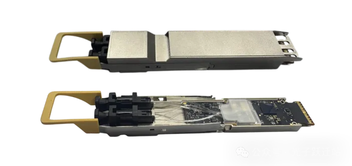
1.6T OSFP DR8 demonstrated at OFC 2026: the upper unit shows the complete module; the lower unit exposes the PCB and optoelectronic devices after cover removal.
Key Takeaway: An optical module is not a standalone “optical chip”, but a high‑speed optoelectronic system packed into thumb‑sized space. It handles electrical signals, laser transmission, signal reception, error correction, system management and thermal dissipation simultaneously. As data rates evolve from 400G to 800G and 1.6T, the core challenge has shifted from “generating laser light” toward per‑bit power consumption, channel density, signal integrity and mass‑production consistency.
AI clusters interconnect tens of thousands of GPUs into one “supercomputer”. Chips continuously exchange parameters, gradients and intermediate computation results. Once inter‑connection bandwidth falls short, costly computing power sits idle waiting for data. Situated between switches, network interface cards (NICs) and optical fibers, optical modules perform the critical conversion: translating high‑speed electrical signals from chips into light for fiber transmission, and converting incoming optical signals back into electrical signals on the far end.
Although it appears as a simple metal box plugged into a port, it internally integrates high‑speed PCB, DSP/CDR, drivers, lasers or modulators, photodetectors, TIAs, optical coupling assemblies, firmware and temperature control. To understand optical modules, memorizing acronyms is far less effective than taking one apart.
| Direction | Signal Path | Module Function |
|---|---|---|
| Transmit (TX) | Switch chip / NIC → Electrical interface → DSP / Driver → Laser / Modulator → Optical fiber | Reshape, encode and modulate; load high‑speed electrical data onto optical carriers |
| Receive (RX) | Optical fiber → Photodetector → TIA → DSP / Electrical interface → Switch chip / NIC | Convert faint optical signals into electric current; amplify, sample and recover raw data |
Common Misconception: The physical propagation speed of light inside optical fiber does not increase with 800G modules. Specifications such as 400G, 800G or 1.6T describe higher data throughput per unit time. Performance gains are achieved via higher symbol rates, advanced modulation formats and additional parallel lanes.
02|Remove the housing: high‑value components reside on the PCB
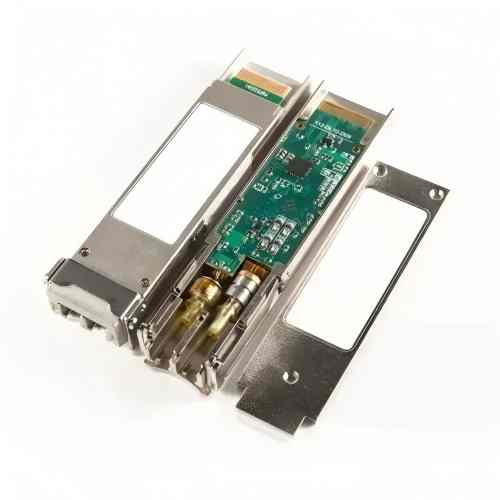
Figure 1: Disassembled 400G QSFP‑DD unit. The metal housing delivers mechanical protection and thermal conduction; the green PCB runs through the entire module, with electrical gold‑fingers and optical ports on opposite ends.
Viewed from outside in, a high‑speed optical module consists of seven functional layers. These components are not simply assembled together: trace length, optical‑fiber bend radius, thermal paths and component placement all determine bit‑error rate and long‑term reliability.
| Component | Function | Engineering Challenges |
|---|---|---|
| Metal housing / Pull tab | Hot‑swap support, EMI shielding, mechanical protection; 800G/1.6T modules often integrate heat‑dissipation fins | Mechanical precision and airflow design |
| High‑speed PCB & Gold fingers | Connect to switch chips or NICs; carry multi‑lane 112G / 224G high‑speed electrical signals | Material loss, crosstalk, routing layout |
| DSP / CDR / Gearbox | Signal equalization, clock data recovery, lane rate conversion, partial FEC functions; acts as the “signal repair station” for high‑speed modules | Power consumption, latency, semiconductor process node |
| Drivers & TIAs | Drive lasers / modulators; amplify tiny photocurrent from photodetectors into usable voltage signals | Bandwidth, noise performance, linearity |
| Optical Transmitter | VCSEL, DML, EML or silicon‑photonic modulator imprints electrical data onto optical carriers | Data rate capability, temperature drift, coupling efficiency |
| Optical Receiver | PIN / APD photodetector converts light back into electric current | Receiver sensitivity, saturation optical power |
| Optical path & interfaces | Lenses, couplers, multiplexers / demultiplexers, FAU, LC / MPO connectors | Insertion loss, lane‑to‑lane consistency |
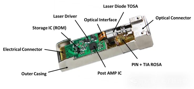
Figure 2: Annotated disassembly of legacy SFP module: Electrical Connector, Storage IC, Laser Driver, Laser Diode TOSA (Transmitter Optical Subassembly), PIN+TIA ROSA (Receiver Optical Subassembly), Optical Connector.
Low‑speed SFP modules traditionally package transmitters as TOSA and receivers as ROSA with clear functional boundaries. For 400G / 800G systems, components shift toward array‑based high‑density integration. Discrete cylindrical subassemblies are gradually replaced by PCB‑proximate optical engines, silicon‑photonic PICs or multi‑channel EML arrays.
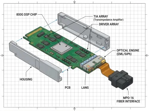
Figure 3: Exploded‑view labeling for an 800G module: DSP CHIP, TIA ARRAY, DRIVER ARRAY, OPTICAL ENGINE (EML/SiPh), PCB, MPO‑16 FIBER INTERFACE.
Key insight from disassembly: An 800G module is not simply a “scaled‑up 400G device”. Within comparable form‑factor volume, it must accommodate faster SerDes interfaces, enhanced signal equalization, denser optical lanes and elevated heat flux. Hence PCB design, packaging, optical coupling and thermal management carry equal importance.
Modern data‑center optical modules widely adopt PAM4 modulation. Unlike NRZ with only two logic levels, PAM4 employs four amplitude levels, encoding two bits per symbol. This delivers higher throughput under equivalent symbol rates. The trade‑off lies in narrower spacing between adjacent amplitude levels: noise, signal reflection, chromatic dispersion and device nonlinearity readily trigger bit errors.
This is where DSP delivers core value: it performs electrical‑domain equalization, clock recovery, lane remapping and bit‑error‑related processing before feeding signals to laser drivers or TIAs. PAM4 widens the transmission highway; DSP plus FEC ensure reliable data delivery.
| Function | Transmit Side | Receive Side |
|---|---|---|
| Electrical domain | Ingest multi‑lane high‑speed SerDes traffic from host equipment | Output recovered high‑speed SerDes data toward host equipment |
| Digital‑analog processing | CDR, equalization, gearbox, FEC coordination, laser driving | TIA amplification, CDR / equalization, signal decision‑making and monitoring |
| Optical domain | Lasers / modulators generate data‑bearing optical signals | PIN / APD detect variations in incident optical power |
| Management | CMIS monitoring for temperature, voltage, bias current, transmit optical power | CMIS monitoring for received optical power, alarms and bit‑error statistics |
Why pursue “DSP‑less” architectures? While DSP improves link margin and interoperability, it is a major contributor to power draw and latency. LPO shifts partial equalization workload onto switch ASICs, leveraging linear analog links to cut module power consumption. Drawbacks include tighter link‑budget constraints and increased complexity for system‑level joint tuning; it fits well for well‑controlled short‑reach scenarios.
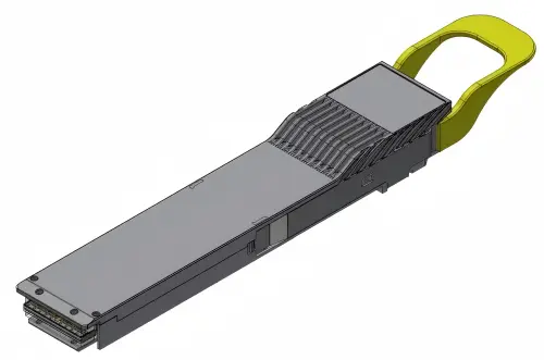
Figure 4: NVIDIA 800G DR4 single‑port OSFP module: four 200G PAM4 electrical lanes map to four 200G optical lanes; 1310 nm single‑mode fiber, maximum reach 500 m, nominal maximum power consumption 18 W.
| Field | Question answered | Meaning in 800G OSFP DR4 |
|---|---|---|
| 800G | Total bandwidth | Aggregate line rate ~800 Gb/s; does not represent a single 800G lane |
| OSFP | Mechanical form‑factor & electrical interface | 8‑lane pluggable form factor with enhanced thermal capacity |
| DR | Reach & fiber type | Datacenter‑Reach; short‑reach single‑mode for data centers, typical target 500 m |
| 4 | Number of optical lanes | Four parallel optical lanes (200G each in this example) |
| MPO‑12/APC | Fiber connector type | Multi‑fiber parallel single‑mode connector; transmit and receive utilize separate fiber cores |
Products labeled “800G” may adopt different internal lane configurations. NVIDIA single‑port 800G DR4 implements 4 × 200G, whereas dual‑port 800G 2×DR4 uses 8 × 100G, housing two independent 400G optical engines within one OSFP shell. Evaluate total line rate first, followed by form‑factor, optical interface and lane count to determine actual module specifications.
| Suffix | General Definition | Typical Distance Range | Scenarios & Optical Implementation |
|---|---|---|---|
| SR / VR | Very short / short‑reach, multi‑mode fiber | Tens of meters up to ~100 m (refer to formal standards) | Intra‑rack / adjacent‑rack deployment; commonly VCSEL + MPO |
| DR | Datacenter short‑reach, parallel single‑mode fiber | Typically 500 m | Intra‑data‑center campus; multi‑fiber parallel MPO interfaces |
| FR | Medium‑reach single‑mode fiber | Typically 2 km; some new Lite variants for 500 m | Inter‑building campus links; wavelength‑division multiplexing with duplex LC connectors |
| LR | Long‑reach single‑mode fiber | Typically 10 km | Campus backbone, metro access networks |
| ZR / ZR+ | Coherent pluggable long‑reach | Starting at ~80 km, extendable to hundreds‑thousands of kilometers | Data‑center interconnection, metro / backbone DWDM transport |
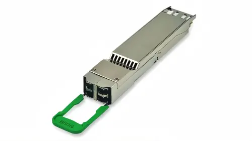
Figure 5: Coherent Silicon‑Photonics 2×400G‑FR4‑Lite. FR‑type solutions multiplex multiple wavelengths onto few fiber cores. Compared with DR parallel optics, FR reduces fiber consumption yet introduces additional multiplexing / demultiplexing and precise wavelength‑control overhead.
DR versus FR: DR leverages abundant fiber cores for straightforward parallel optical paths and flexible lane breakout capability. FR applies wavelength‑division multiplexing to conserve fiber resources, better suited for distance‑extended deployments with constrained fiber infrastructure. Neither architecture is universally superior; selection depends on fiber availability, reach requirement, power budget, cost and operation‑maintenance workflows.
| Aggregate Rate | Common Form Factors | Typical Lane Organization | Industry Status in 2026 |
|---|---|---|---|
| 100G | QSFP28 | 25G NRZ or newer single‑lane alternatives | Mature mass deployment; access networks, servers and legacy data centers |
| 400G | QSFP‑DD / OSFP / QSFP112 | Combination of 50G / 100G per lane | Mainstream deployed for modern data‑center switching fabrics |
| 800G | OSFP / QSFP‑DD800 | 8 × 100G or 4 × 200G | Large‑scale adoption within AI clusters; significant platform‑specific variations |
| 1.6T | OSFP / QSFP‑DD1600 | Mainstream roadmap: 8 × 200G; forward‑looking exploration: 4 × 400G | Accelerating productization and system validation; IEEE standards still under development |
IEEE 802.3df standardization for 800G completed in 2024. As of August 2026, IEEE P802.3dj for 1.6T remains within working‑group discussion and balloting cycles. Nevertheless, industry development does not wait for final ratification: multiple vendors have demonstrated or shipped 1.6T OSFP modules built upon draft specifications together with OIF 224G electrical interfaces. It is critical to distinguish “commercially available products” from “fully finalized official standards”.
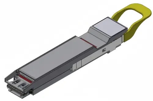
Figure 6: Internal schematic of NVIDIA 1.6T dual‑port OSFP: eight 200G PAM4 electrical lanes; optical side implements two independent 800G DR4 ports with two MPO‑12/APC connectors, supporting maximum 500 m single‑mode links.
200G per‑lane signaling enables 1.6T implementations within existing 8‑lane form‑factors, yet imposes stricter requirements for DSPs, lasers, photodetectors, packaging and test procedures. Broadcom released its 3‑nm Sian3 DSP in 2025 targeting reduced 1.6T module power consumption. At OFC 2026, Broadcom further unveiled 400G‑per‑lane optical DSP silicon, enabling potential migration from 8 × 200G toward 4 × 400G optical lanes for 1.6T and paving the path for 3.2T generations. This advanced configuration remains cutting‑edge exploration and is not representative of all current‑generation 1.6T modules.
| Technology Roadmap | Advantages | Drawbacks | Target Application Scope |
|---|---|---|---|
| Discrete EML/DML Optics | Independently optimized lasers, photodetectors and optical paths with proven performance trajectories | Large component count; complex assembly‑alignment; rising cost & power consumption as lane count scales | 800G / 1.6T short‑to‑medium‑reach single‑mode links |
| Silicon Photonics (SiPh) | Integrate modulation, beam‑splitting and multiplexing functions onto silicon‑based PICs, favorable for high‑volume manufacturing | External light‑source dependency; persistent challenges for optical coupling, packaging and production yield | DR / FR applications, highly‑integrated optical engines |
| LPO / LRO | Remove or simplify on‑module DSP circuits for lower power consumption and reduced latency | Link‑budget margin and interoperability heavily rely on system‑level co‑design | Well‑controlled short‑reach scenarios, dedicated switch platforms |
| CPO / NPO | Place optical engines in close proximity to switch ASICs to shorten power‑hungry high‑speed electrical traces | Challenges around field maintainability, laser‑source supply, packaging, thermal dissipation and complete industrial ecosystem | Long‑term solution for ultra‑high port‑density environments |
.webp)
Figure 7: Physical photograph of silicon‑photonic optical engine. Large DSP / PHY chips sit near the electrical side; photonic integrated circuits and coupling structures concentrate at the optical connector end. High integration reduces discrete optical parts and active alignment steps.
In the near‑term, pluggable modules retain strong advantages for field maintainability and mature supply‑chain ecosystems. LPO / LRO architectures aim to partially cut DSP‑related overhead. CPO represents a more fundamental reconstruction of switch internal hardware. These technologies are not mutually‑exclusive replacements. They will coexist according to transmission‑distance requirements, port density targets, power budgets and operation‑maintenance constraints.
| Seven key questions | Practical verification checklist |
|---|---|
| 1. Host‑equipment compatibility | Confirm form‑factor, protocol, line rate, host‑side FEC capability and CMIS version. OSFP and QSFP‑DD cannot be arbitrarily interchanged based solely on physical connector fit. |
| 2. Actual transmission distance | Select SR / DR / FR / LR / ZR according to worst‑case link loss; do not trust nominal reach values in isolation. |
| 3. Fiber core consumption | MPO parallel optics consume multiple fiber cores; LC‑based wavelength‑multiplexed interfaces save fiber count but add optical‑path complexity. |
| 4. Lane breakout support | Verify support for breakout configurations: e.g. 800G to 2 × 400G / 4 × 200G / 8 × 100G; also validate fiber polarity. |
| 5. Power and thermal sufficiency | High‑power modules demand matching port power classes, airflow, heat sinks and ambient operating temperature. |
| 6. Interoperability & coding matching | Cross‑check vendor qualification reports, FEC modes, firmware whitelists, wavelengths and connector end‑face types. |
| 7. Monitoring capability | Leverage CMIS / DOM telemetry to continuously monitor temperature, voltage, bias current, transmit / receive optical power and alarm events. |
Common Pitfall: Mechanical insertion compatibility does not guarantee functional link establishment. Identical outer form‑factors can hide differing lane‑mapping schemes, FEC profiles, wavelength assignments, fiber polarity and thermal ratings. Prior to procurement and commissioning, always cross‑reference switch‑ASIC port capabilities, module datasheets and fiber‑cabling infrastructure.
Opening up an optical module reveals overlapping disciplines: communications engineering, optics, analog circuits, digital signal processing, packaging science and thermal design. The metal shell serves only as an interface, and PCB merely acts as substrate. Real performance is determined by end‑to‑end coordination across the complete link spanning host SerDes to fiber end‑face.
From 400G through 800G toward 1.6T, clear industry trends emerge: rising per‑lane signaling rates, accelerating adoption of silicon‑photonic highly‑integrated optical engines, DSP migration toward advanced process nodes, alongside LPO and CPO exploring low‑power system‑level architectures. Future competition extends beyond simply achieving higher raw line rates. Differentiation will center on per‑bit power efficiency, mass‑production yield, long‑term reliability and multi‑vendor end‑to‑end interoperability.
One‑sentence takeaway: Optical modules do not increase the physical travel speed of light. They enable vastly larger volumes of data to traverse optical fiber with reduced energy expenditure, suppressed bit‑error rates and elevated port density.

APEX GROUP LIMITED
Phone: 85298213834
WhatsApp: 85298213834
Email: Info@apexallinone.com